
By Robin WenReviewed
High-Purity Silicon: Solar and Chips Differ
How high-purity silicon becomes solar cells and chips, why Chinese production clusters matter, and what purity figures leave out.
On this page
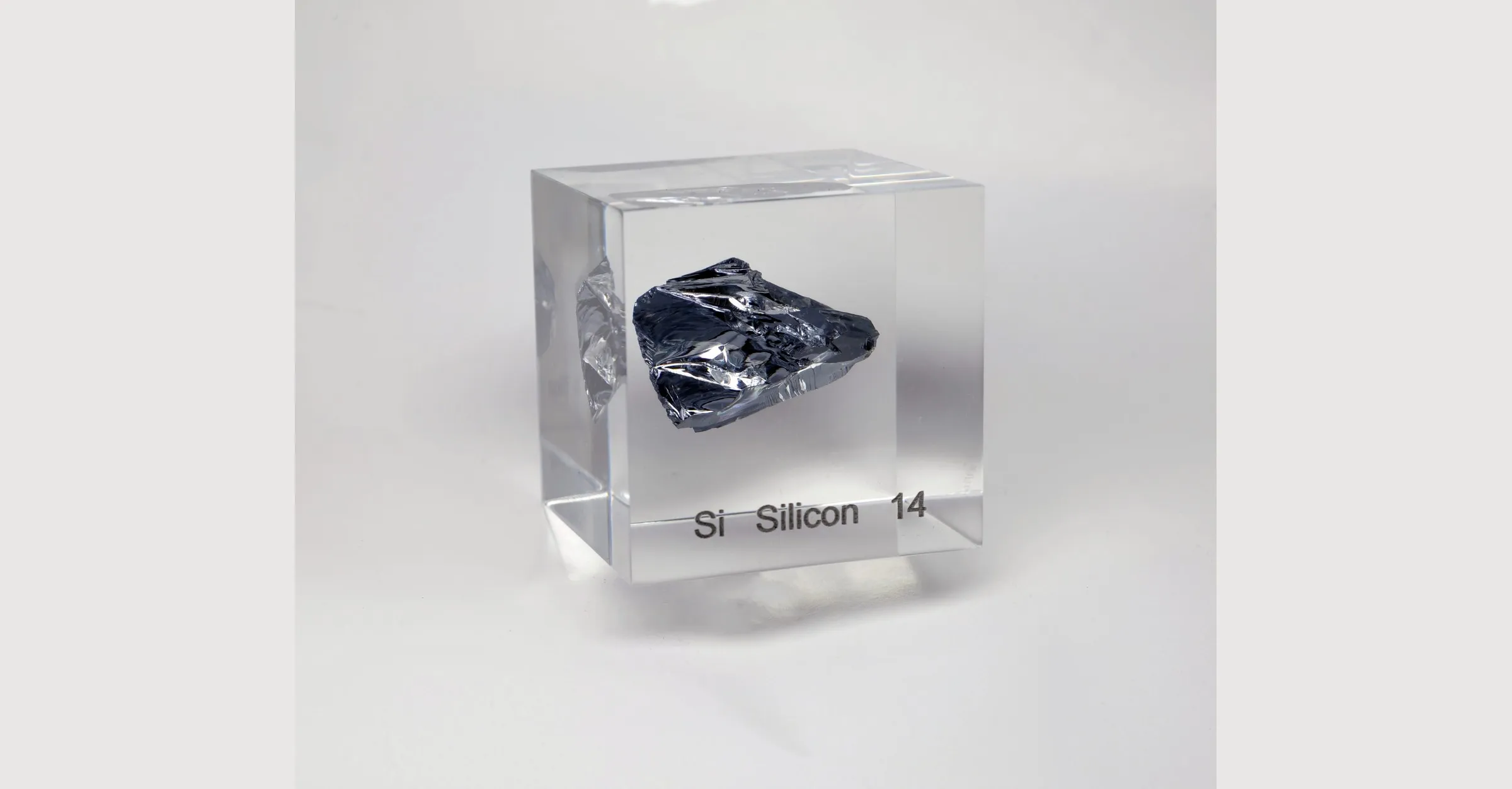
High-purity silicon is silicon refined to control impurities for demanding applications such as solar cells and semiconductor devices. Silicon metal and polysilicon are the same element at different points in that chain. This page focuses on bulk silicon feedstock: how it is purified, what the downstream customer needs, and why production locations matter.
The material may be destined for a solar wafer or a semiconductor wafer. The number of nines matters, but it does not answer the questions that determine whether the material is usable: which impurities are controlled, how consistent is the product, what is its surface condition, and has the customer qualified it for the next process?
That distinction matters because the same supply chain begins with ordinary silicon metal and ends in products with radically different tolerance for defects. It also explains why China became so important in polysilicon without making every Chinese product interchangeable with every other product.
Silicon metal is the first product in the chain
The chain is easier to understand as a sequence of transformations. It begins with a silica feedstock; high-purity quartz is treated separately because its grades and its supply chain are not silicon’s.
Quartz or other silica feedstock
        ↓
Metallurgical-grade silicon (MG-Si)
        ↓
Chlorosilane purification and silicon deposition
        ↓
High-purity polysilicon
        ↓
Ingots and wafers
        ↓
Solar cells, modules or semiconductor devices
Quartz is mainly silicon dioxide. In a submerged-arc furnace, carbon removes the oxygen at high temperature and produces metallurgical-grade silicon metal. PVEducation describes MG-Si as roughly 98% pure, while Wacker gives a range of roughly 98% to 99% for its initial silicon product. That is enough for many metallurgical uses, but not enough for photovoltaic or electronic substrates.
Metallurgical-grade silicon (MG-Si) undergoes chemical purification to produce high-purity polysilicon. In the route described by PVEducation, MG-Si reacts with hydrogen chloride to form trichlorosilane, a volatile silicon compound. Distillation separates the trichlorosilane from compounds carrying unwanted impurities. The purified compound is then decomposed in a deposition reactor, leaving silicon on heated starter rods.
Polysilicon from chemical deposition is feedstock for crystal growth. Wacker’s process description describes breaking rods into chunks and cleaning their surfaces for semiconductor applications. The chunks are starting material for solar cells and semiconductor wafers, rather than finished devices.
This is why “silicon” is an unsafe shortcut. Silicon metal, polysilicon, a silicon ingot and a silicon wafer are different products at different points in the chain.
Purity and crystal structure answer different questions. “High-purity” describes impurity control; “polycrystalline” and “monocrystalline” describe the arrangement of crystals. High-purity polysilicon can be feedstock for growing a single-crystal ingot. PVEducation’s Czochralski silicon explanation describes single-crystal growth and notes that CZ wafers serve solar and integrated-circuit production. Buying polysilicon therefore does not mean the finished wafer or panel must be multicrystalline.
From feedstock to applications
For crystalline-silicon photovoltaics, the material becomes the semiconductor in the solar cell, where absorbed light generates charge carriers that can be collected as electric current. PVEducation’s solar-cell structure explanation describes that function. Polysilicon first passes through ingot growth and wafer making; the wafer then undergoes cell processing, and cells are assembled into modules. A module assembler is downstream of these transformations, rather than the defining buyer of raw polysilicon.
In microelectronics, the feedstock becomes a semiconductor wafer on which devices are fabricated. Hemlock’s electronics page describes its polysilicon becoming wafers and integrated-circuit chips, with end uses including computers and mobile phones. These end products explain demand, but a phone manufacturer and a silicon crystal grower have different purchasing tasks.
My practical distinction is between the immediate processing customer and the final market. A crystal grower evaluates feedstock against its process; an investor or electronics brand may instead need to understand an upstream dependency. Neither task is served well by a list that places raw polysilicon, wafers and finished chips in one product category.
Why a trace impurity can matter
Purification is not cosmetic. Silicon is used because its electrical behavior can be controlled. Foreign atoms and structural defects can change that behavior in ways that affect carrier lifetime, resistivity, device performance and yield.
PVEducation notes that transition-metal contamination introduces electrically active levels in the band gap and can increase recombination. It also notes that boron and phosphorus concentrations in metallurgical silicon are too high to allow suitable compensation procedures. The practical meaning is simple: an impurity is not merely a reduction in a purity percentage. Its identity, concentration and location matter.
The surface matters too. Wacker describes additional cleaning of semiconductor-grade polysilicon chunks because surface contamination can affect later processing. A supplier that reports a bulk purity figure but says little about surface metals, particle control, packaging or handling is leaving out part of the specification.
This is the first useful rule for a buyer or analyst: do not treat “99.999999%” as a complete product description. Ask what is included in the analysis, which impurities are controlled, whether the figure refers to bulk material or surface condition, and what test method supports it.
Solar grade and electronic grade are different jobs
Solar-grade and electronic-grade polysilicon are related, but they are not simply two labels on one universal ladder.
Solar cells can tolerate higher impurity levels than integrated-circuit fabrication, as PVEducation’s refining-silicon explanation states. For a buyer, my recommendation is to compare the impurity limits and qualification requirements for the intended process rather than infer suitability from a grade label alone.
In its process guide updated in September 2020, Bernreuter Research gives indicative ranges of 7N to 8N for multicrystalline solar material, 9N to 10N for monocrystalline solar material, and 10N to 11N for electronic-grade material. The notation counts nines in the purity percentage: the guide illustrates 7N as 99.99999%. Those ranges are historical orientation, not a current universal standards table. Different producers and customers can define grades through a wider package of requirements than the headline purity number suggests.
The commercial difference is visible in qualification. Hemlock Semiconductor says it pursued IATF certification in response to requirements from semiconductor customers serving the automotive industry. That does not make IATF certification a universal requirement for polysilicon. It does show that a supplier’s value can depend on quality systems, auditability and process consistency as well as chemical purity.
A useful comparison is this:
| Question | Solar-grade material | Electronic-grade material |
|---|---|---|
| Main downstream use | Solar cells and modules | Semiconductor wafers and devices |
| Tolerance for impurities | Higher than in integrated-circuit production, depending on the process | Much tighter and more process-specific |
| Commercial proof | Crystal-growth performance, cell efficiency and consistency | Defect control, electrical behavior, traceability and customer qualification |
| Key mistake to avoid | Treating every solar-grade product as equivalent | Treating a purity claim as proof of fab qualification |
The table is a screening model, not a substitute for a customer specification.
Siemens and fluidized-bed reactor processes
The Siemens process produces high-purity polysilicon through chemical purification followed by chemical vapor deposition.
MG-Si is ground and reacted with hydrogen chloride. The resulting trichlorosilane is distilled. In Wacker’s process description, accessed in October 2026, the deposition step uses approximately 1,000°C and thin heated silicon rods. Silicon deposits on the rods, which are later broken into chunks.
The process is expensive in energy and equipment, but it has a long operating history and can produce material for demanding applications. Bernreuter’s account also highlights the less visible part of the route: by-products such as silicon tetrachloride can be recycled through hydrochlorination, and process improvements have reduced costs over time.
Fluidized-bed reactor (FBR) technology takes a different path. Silicon-containing gas and hydrogen flow through a bed of small silicon seed particles. Silicon deposits on the particles, which grow into granules that can be withdrawn continuously. In its September 2020 guide, Bernreuter describes lower reactor electricity consumption for a monosilane-fed FBR than for heating a conventional rod reactor, alongside fluid-dynamics, contamination-control and silicon-dust challenges. This is a process comparison, not evidence of present-day market share or a universal whole-plant cost advantage.
My comparison would therefore start with electricity, throughput, product form and contamination control, then ask what the customer accepts.
Why China became the centre of the solar chain
China’s solar manufacturing position combines power economics with a wider production system.
The IEA’s 2022 analysis found that China’s share of the major solar-PV manufacturing stages, including polysilicon, ingots, wafers, cells and modules, exceeded 80% at that time. It also reported that electricity accounted for more than 40% of polysilicon production costs in its analysis. Those figures explain why power matters, but not why a production system became so concentrated.
The wider explanation includes large domestic demand, rapid capacity expansion, supplier learning, equipment localisation, chemical integration and industrial clustering. Bernreuter describes Chinese producers benefiting from low-cost equipment, capital, raw materials, labour and electricity, while the IEA links China’s position to industrial policy and the scale of its domestic PV market.
A producer also benefits when related operations are close together. Industrial silicon, chlorosilanes, power generation, polysilicon deposition, wafer production and chemical recovery can be connected through infrastructure, contracts and technical labour. Tongwei’s own description of Sichuan Yongxiang presents this kind of integration, connecting chemical operations with high-purity crystalline silicon. That is a company description, not an independent audit, but it illustrates the industrial logic.
Geographic concentration is a supply-chain exposure for polysilicon. The IEA’s 2022 assessment reported that Xinjiang accounted for 40% of global polysilicon manufacturing. That figure should not be reused as a current market-share claim without an updated source. My interpretation is that low cost and abundant supply do not, by themselves, resolve geographic, electricity, trade, traceability or policy risks.
China’s silicon clusters connect different stages
Leshan in southwestern China’s Sichuan province illustrates how an industrial belt can reduce the distance between purification, crystal growth and equipment supply. In a February 2024 Securities Daily report republished by People’s Daily Online, reporters describe Yongxiang and GCL silicon-material operations near JinkoSolar and Jingyuntong facilities in Wutongqiao. Jingyuntong’s local deputy general manager said proximity to upstream Yongxiang helped reduce transport, warehousing and logistics costs. The report also describes the area’s silicon research history, hydropower resources and infrastructure support. This is a concrete cluster mechanism: expertise and shared infrastructure accompany supplier proximity.
Other locations illustrate different parts of the chain:
| Production area | Documented industrial relationship | What the relationship tells a reader |
|---|---|---|
| Baotou, Inner Mongolia, northern China | An October 2026 Inner Mongolia Daily report lists Tongwei, Daqo, GCL, Shuangliang and other PV companies established in the city | The cluster spans multiple businesses; the company list is not a list of interchangeable feedstock suppliers |
| Baoshan, Yunnan, southwestern China | An April 2024 report on the municipal government portal describes Tongwei’s high-purity silicon operation near LONGi’s single-crystal rod production | Polysilicon supply and downstream crystal growth can develop in the same industrial park |
| Guangyuan, Sichuan | Tongwei’s base description identifies its Guangyuan project as industrial silicon | A group’s regional investment may concern upstream silicon metal rather than purified polysilicon |
The Baoshan report links the city’s industrial strategy to mineral and hydropower resources and describes efforts to extend the chain into wafers, cells and modules. The Baotou report documents a multi-company cluster; it does not establish every plant’s power tariff or customer approvals. These examples explain industrial relationships, not current output rankings.
Regional power resources can help explain investment, but a province’s hydropower reputation is not batch-level evidence of a product’s electricity supply or carbon footprint. For procurement, ask for the specific plant, product and documentation. My reading is that a useful supply map should show the process stage and qualified product at each location, rather than aggregating every project labelled “silicon” into one capacity total.
The questions that matter when screening a supplier
A serious first-pass review should ask at least seven questions:
- Which downstream grade is being offered? Solar-grade, electronic-grade and intermediate descriptions are not interchangeable.
- Which impurities are controlled? Request the impurity list, limits, test method and whether the result is bulk or surface measurement.
- What physical form is supplied? Rods, chunks and granules can affect loading, crystal growth and handling.
- Which process route is used? Siemens and FBR have different energy, form, contamination and operating characteristics.
- How consistent is the output over time? A single certificate does not show lot-to-lot stability.
- What qualification evidence exists? Customer approvals, audit systems, traceability and process-change controls may matter more than a marketing purity figure.
- What is the plant’s cost and location logic? Power price, energy mix, chemical integration, logistics and downstream proximity all affect resilience.
A comparison that names the grade, the impurity profile and the qualification record is checkable; one that names only a headline percentage is not. A supplier with a higher headline purity is not automatically better if the impurity profile does not match the customer’s process, the product is inconsistent, or the qualification record is absent.
High-purity silicon: a working definition
High-purity silicon is refined silicon whose impurity profile and process consistency are controlled tightly enough for a specified downstream use. The phrase covers more than one grade and more than one market. It does not, by itself, identify a universal purity threshold, a production route or a qualified supplier.
It is one of five material guides on this site; the full set is indexed at industrial materials. That is also the right way to read the industry. Purity is the visible number. The industrial value sits underneath it: chemical purification, reactor control, surface treatment, low-cost power, scale, traceability and customer qualification. When those pieces move together, a silicon producer can supply a wafer chain. When one breaks, the number of nines may not rescue the product.
Methodology
Technical descriptions draw on PVEducation and supplier process pages. Bernreuter’s purity ranges and FBR discussion are dated to its 2020 guide; IEA figures are dated to its 2022 report. They explain technical and economic relationships rather than current market shares. Regional examples come from dated reporting and company descriptions, not plant audits or a complete national inventory. Company disclosures establish what a supplier claims, not independent proof of customer qualification. Current purchasing decisions require product-specific specifications, testing and traceability evidence.
Sources
- International Energy Agency, Solar PV Global Supply Chains (2022). https://www.iea.org/reports/solar-pv-global-supply-chains/executive-summary
- PVEducation, “Refining Silicon”. https://www.pveducation.org/pvcdrom/manufacturing-si-cells/refining-silicon
- Wacker Chemie, “Polysilicon: From silicon to value”. https://www.wacker.com/cms/en-us/about-wacker/profile-and-organization/wacker-polysilicon.html
- Bernreuter Research, “Polysilicon Production Processes”. https://www.bernreuter.com/polysilicon/production-processes/
- Tongwei, “High-purity Crystalline Silicon”. https://en.tongwei.cn/silicon.html
- Sichuan Yongxiang / Tongwei. https://en.si.tongwei.cn/
- Hemlock Semiconductor, IATF certification announcement. https://www.hscpoly.com/hemlock-semiconductor-becomes-first-polysilicon-manufacturer-worldwide-to-earn-iatf-certification/
- PVEducation, Czochralski silicon (technical explainer). https://www.pveducation.org/pvcdrom/manufacturing-si-cells/czochralski-silicon
- PVEducation, solar-cell structure (technical explainer). https://www.pveducation.org/pvcdrom/solar-cell-operation/solar-cell-structure
- Hemlock Semiconductor, electronics applications (company description). https://www.hscpoly.com/markets-technologies/electronics/
- Securities Daily, Leshan cluster reporting, republished by People’s Daily Online (26 February 2024). http://sc.people.com.cn/n2/2024/0226/c345458-40756604.html
- Baoshan municipal portal, upstream silicon industrial chain (18 April 2024; republished reporting). https://www.baoshan.gov.cn/info/5730/9975554.htm
- Inner Mongolia Daily, silicon conference and Baotou cluster (12 October 2026; People’s Daily Online republication). http://nm.people.com.cn/n2/2026/1012/c196667-41719089.html